The novelty of this paper is to present the design techniques that lead to high performance memory controllers. For details on this termination scheme refer to DDR533 Memory Design for Two-DIMM Unbuffered Systems located on Microns web site.

Ddr5 How Faster Memory Speeds Shape The Future Edn Asia
3 DDR Interface Design Implementation A Lattice Semiconductor White Paper Where DRAM Gets Used 43B Units PC 48 Other Servers 3 14 Peripherals 4 Consumer 10 Graphics 9 Comm 12 Figure 1 Market analyses indicate that DDR is currently utilized in over 50 of all electronic systems and usage is expected to increase to 80 over the next.

. Even within the same application space design teams creating SoCs that use the same CPUs and have similar functions often use the DDR interface differently. Furthermore the mixed signal aspect of the architecture requires careful designing or selection of IO cells to mitigate power switching noises and manage signal integrities for the interface channel of the whole system. For example designers using DDR IP like Synopsyss uMCTL2 memory controller have about 70.
The design engineer can no longer simply connect data and address lines and expect to have a robust high-speed memory interface. This is an eye diagram generated at full speed when the DQ is running at 533 MHz and the FPGA is driving into the DDR3 memory see Figure 7. This paper deals with the FPGA-implementation of a high-speed interface for DDR SDRAMs.
The major feature of ddr interface compared to a single data rate sdr one is to use both rising and falling edges of a clock to transfer data which allow it. International Journal of Engineering Research Technology IJERT ISSN. The newest members of the Fast Cycle RAM FCRAM series are 256 Mbit high-speed memories that incorporate the double data rate DDR SDRAM interface.
Further complicating the implementation of a DDR design is the need to handle and pre-process strobe signals as opposed to generic clock signals. DDR IP has evolved to be adaptable or configurable to different applications constraints. Zhao Published in ASICON 11 December 2009 Computer Science As the bandwidth requirement increases Double Data Rate DDR interface is becoming very commonly used in many types of memories such as DDR IIIIII DRAM RLDRAM III QDR IIIII SRAM etc.
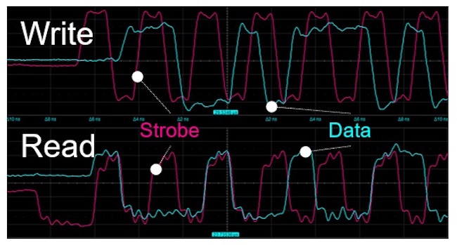
For lightly and medium loaded memory subsystems 418 chips the compensation cap method is not as beneficial. DDR3 533MHz Eye Diagram click on image to enlarge. During DDR3 memory layout the interface is split into the command group the control group the address group as well as data banks 01234567 clocks and others.
DDR SDRAM Main Controller Block Before it is operational the DDR SDRAM memory. Everything starts with the recommended high speed PCB design rules for routing DDR3 in groups. DDR3 Memory Design Rules and Signal Groups.
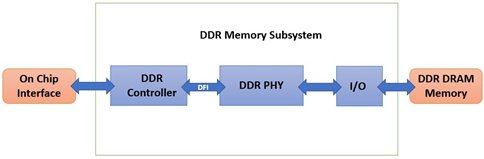
Because numerous memory topologies and interface frequencies are possible on the DDR interface Freescale highly recommends that the board designer verify through simulation all aspects signal integrity electrical timings and so on before PCB fabrication. DFI 50 Specification for High-Speed Memory Controller and PHY Interface AUSTIN Texas May 2 2018 The DDR PHY Interface DFI Group today. Designers are increasingly turning to source-synchronous interconnects that demonstrate transfer rates of 1 billion transitionssec at distances of 5m and greater.
4 Issue 07 July-2015 Design and Implementation of High Speed DDR SDRAM Controller on FPGA Veena H K Dr. Off-chip high density low-cost DDR memory technology has now. ASIC chip die package board traces and memory module.
Traditional interfaces limit interconnect speed to less than 250 MHz and pc-board-interconnect length to approximately 5 in. The DDR SDRAM uses DDR architecture to achieve high-speed operation. The major feature of DDR interface compared to a single data rate SDR one is to use both rising and falling edges of a clock to transfer data which allow it to provide two times the throughput at the same clock frequencyThe high speed up to 16 GHz for DDR III nature and complex timing issues take the most attention for designers of ASIC chips with DDR memory controllers.
A H Masthan Ali MTech Student Department of ECE Associate Professor Department of ECE Sambhram Institute of Technology Bangalore Sambhram Institute of Technology. Figure 4- FPGA As Memory Controller. Several examples of source-synchronous technology exist.
The major feature of ddr interface compared to a single data rate sdr one is to use both rising and falling edges of a clock to transfer data which allow it to provide two times the throughput at the same clock frequencythe high speed up to 16 ghz for ddr iii nature and complex timing issues take the most attention for designers of asic. Is a random access memory interface technology used for high bandwidth storage of the. High speed DDR memory interface design B.
Design of High Speed DDR3 SDRAM. Termination method for improving eye apertures for a heavily loaded system 18 memory chips. The DDRAM is based on 2n pre-fetch architecture that can achieve two data words per clock pulse at the IO pins for a single read or write access.
They are designed for high-performance. In addition to compliance testing Rohde and Schwarz DDR test solutions help you efficiently verify and debug your design at the board and system level. Also be sure to consult the latest errata.
We aim to achieve a performance in terms of bandwidth comparable to ASIC implementations. As part of the overall design DDR memory controller and memory devices also need to properly work in the presence of other high-speed interfaces or even wireless signals. These FPGAs achieve the industrys highest external memory interface speeds.
First of all we compile the specific hardware. Abstract Signal integrity for high speed DDR memory design at the printed circuit board PCB level is very essential and important for making a robust design This paper describes how simulation tools can be helpful for choosing best termination method and other signal integration parameter along with the design process A Simulation tool Hyperlynx has been used for high. Value of DDR Memories from Market Eye Good Balance of High DensityLow Cost and Small PackageHigh SpeedLow Power Flash offers high density and nonvolatility but very slow write speeds SRAM offers low standby power high-speed operation and requires no refresh but costs increase due to large die sizes.
Ddr Memory And Interface Design Memory performance is a critical part of achieving system performance in many applications.

Nine Dot Connects Ddr3 Ddr4 Lpddr4 Design And Layout Services Nine Dot Connects 9ot Ndc Ninedotconnects

Ddr Memory Interface Basics 2017 07 05 Signal Integrity Journal
Ddr Memory Interface Basics 2017 07 05 Signal Integrity Journal
Fly By Topology Routing For Ddr3 And Ddr4 Memory Pcb Design Blog Altium

Figure 1 From Design And Implementation Of High Speed Ddr Sdram Controller On Fpga Semantic Scholar
Ddr Memory Interface Basics 2017 07 05 Signal Integrity Journal
Ddr Ip Hardening Overview Advance Tips

Pin On Memory
0 comments
Post a Comment